- 5 VNominal supply
- 3Redundant IMUs
- 36 × 36 mmBoard size
- 2 × CANDroneCAN buses
Overview
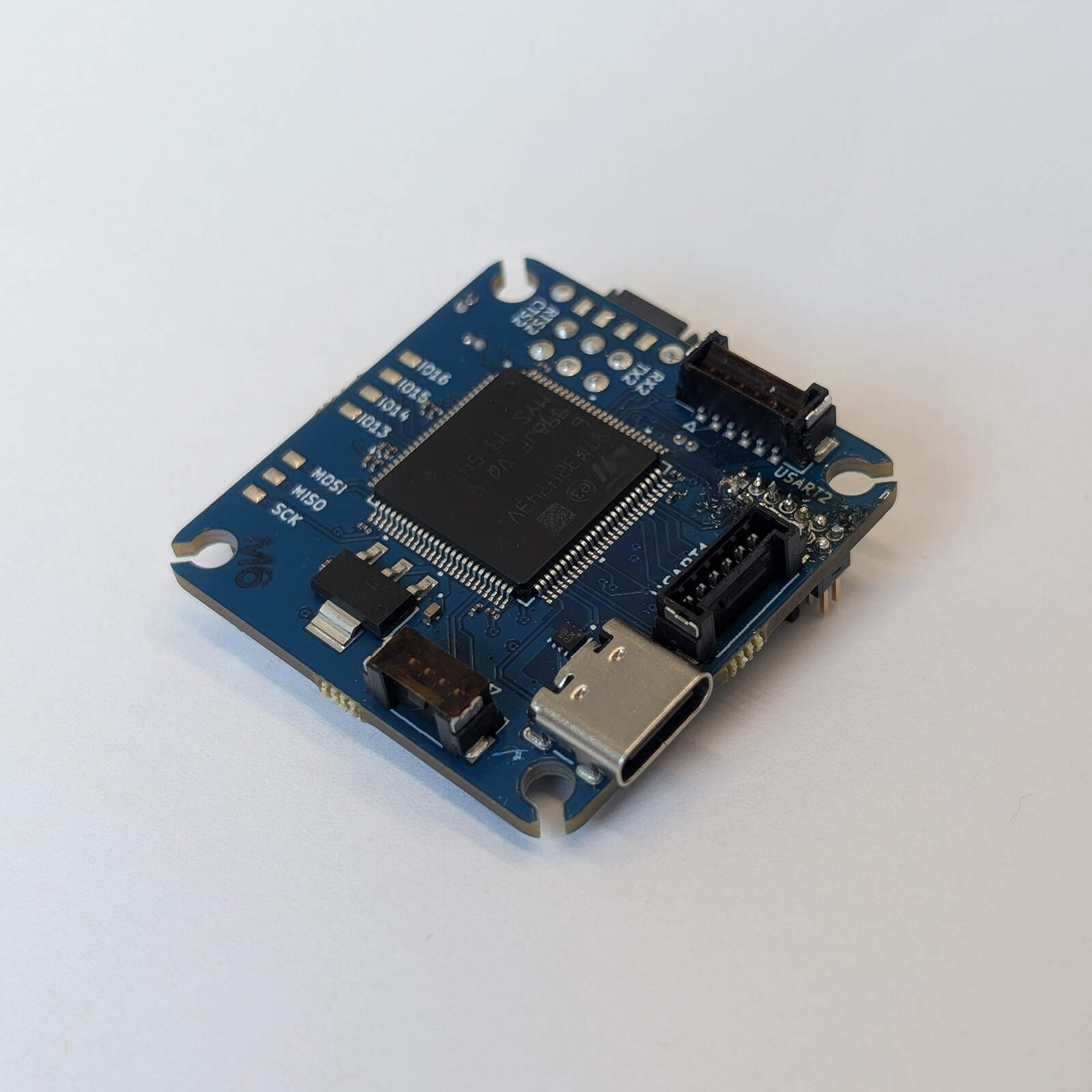
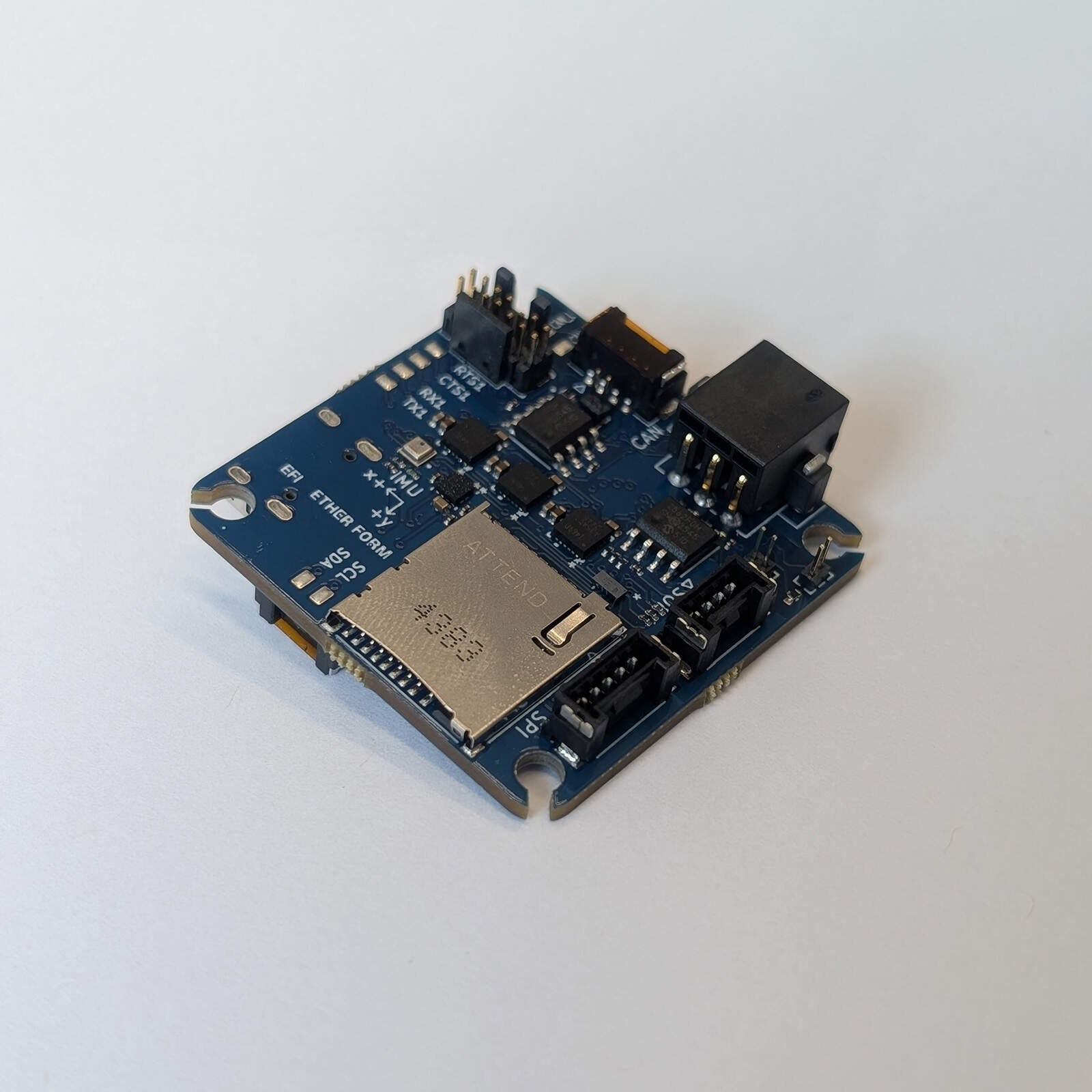
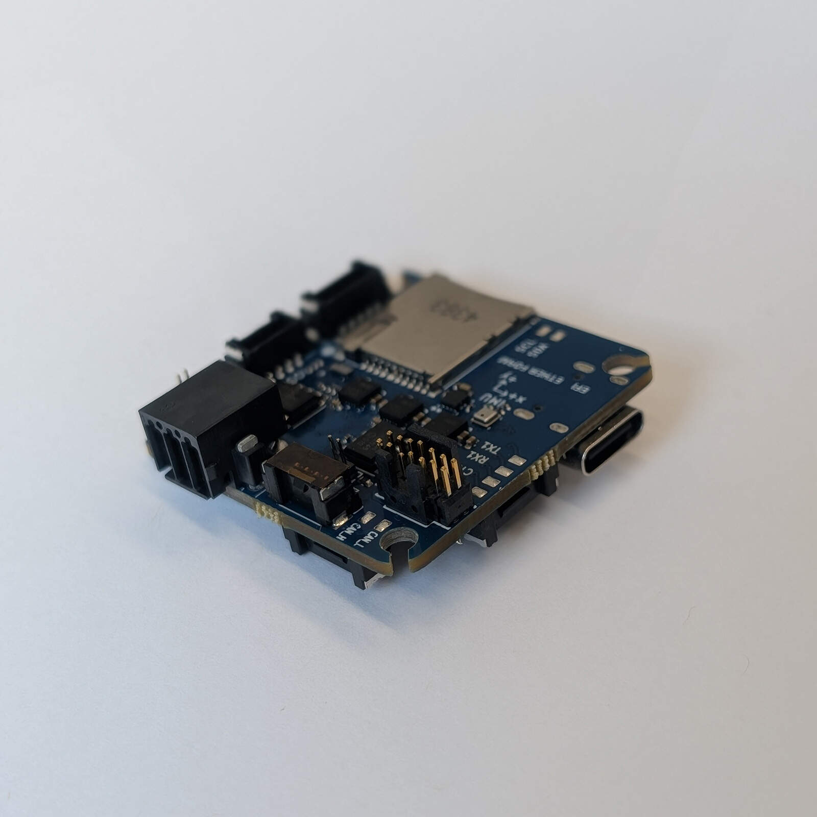
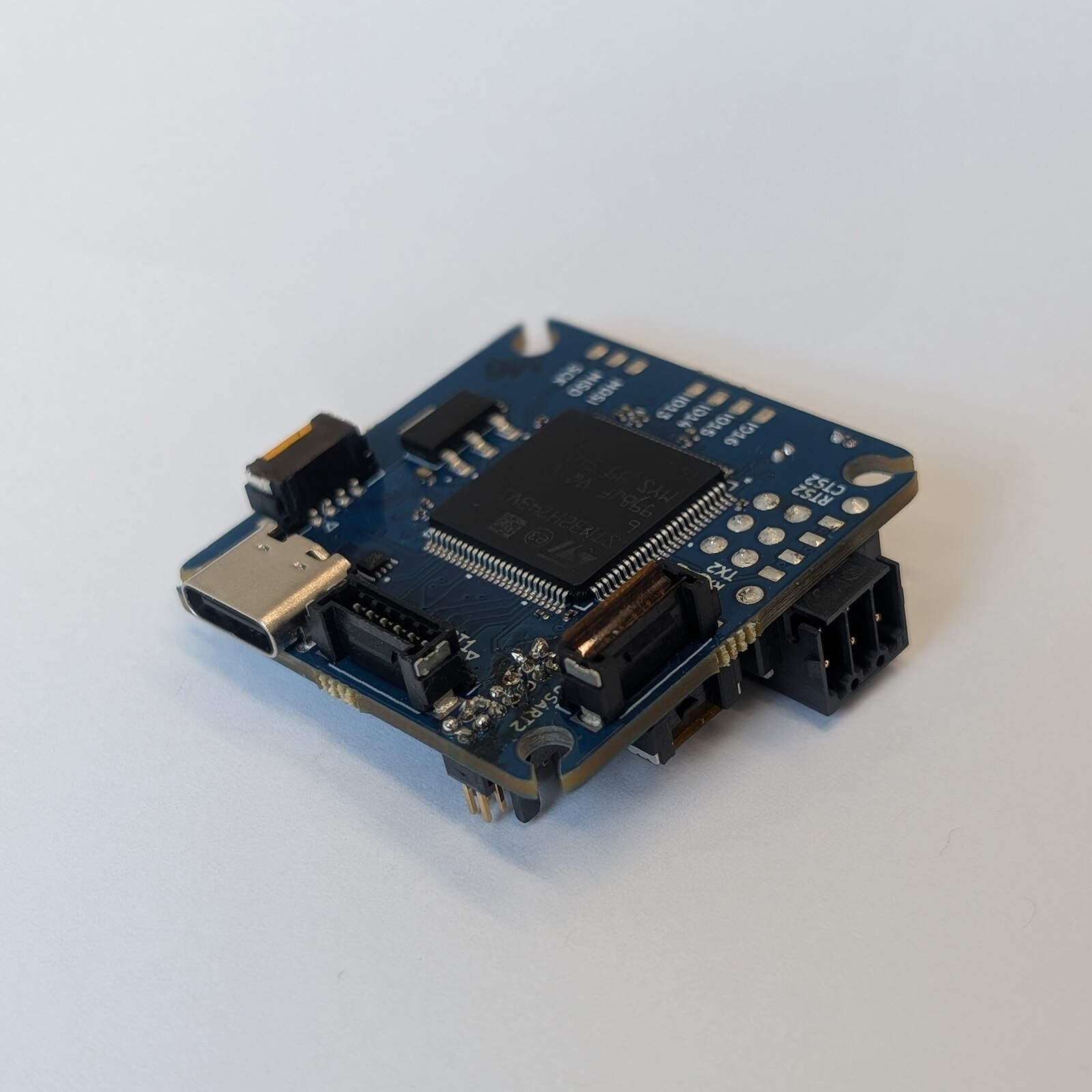
The FC3 is a compact, high-performance flight controller for autonomous and remotely piloted aircraft. It is built around the STM32H743VIT6 microcontroller and combines three ICM-40609-D inertial measurement units for redundant inertial sensing, an IIS2MDC magnetometer for heading and an ENS220 barometer for altitude. A micro SD card socket provides onboard data logging. Two CAN buses carry DroneCAN (UAVCAN) traffic to actuators and sensors, and the board also exposes SPI, I²C, two USARTs, four GPIO, USB and a debug port, either on connectors or on solder pads. The FC3 is intended to run the PX4 autopilot; the PX4 board target for it is efi/revA.
Key features
- STM32H743VIT6 Cortex-M7 microcontroller at 480 MHz, 2 MB flash, 1 MB RAM
- Three ICM-40609-D IMUs (accelerometer and gyroscope) on SPI4 for redundant inertial sensing
- IIS2MDC 3-axis magnetometer and ENS220 barometric pressure sensor on I²C
- Micro SD card socket (4-bit SDMMC) for data logging
- 2 × CAN (FDCAN with MCP2562FD transceivers), each with a selectable 120 Ω termination
- Interfaces: 1 × SPI, 1 × I²C, 2 × UART (USART with RTS/CTS flow control) and 4 × GPIO on connectors with matching solder pads, plus USB Type-C (full speed)
- STDC14 debug and programming connector with a USART3 serial console
- PX4 board target (efi/revA) with DroneCAN support
- Single 5 V supply (4.5 to 5.5 V)
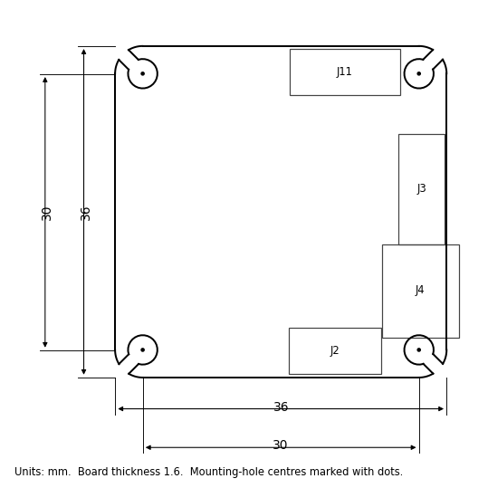
- 36 × 36 mm board, 30 × 30 mm mounting pattern
Technical specifications
| Parameter | Value | Unit |
|---|---|---|
| Electrical | ||
| Nominal supply voltage | 5 | V |
| Minimum supply voltage | 4.5 | V |
| Maximum supply voltage | 5.5 | V |
| Typical input current | 46.6 | mA |
| Maximum input current | 820 | mA |
| Typical power consumption | 233 | mW |
| Processor and memory | ||
| Microcontroller | STM32H743VIT6 | |
| CPU clock (PX4 board configuration) | 480 | MHz |
| Flash / RAM (device) | 2 / 1 | MB |
| Interfaces | ||
| CAN buses (FDCAN, MCP2562FD transceivers) | 2 | |
| USART with RTS/CTS | 2 | |
| SPI (external) | 1 | |
| I²C (external) | 1 | |
| GPIO | 4 | |
| Micro SD (4-bit) | 1 | |
| USB | Full speed, Type-C | |
| Sensors (manufacturer typical values) | ||
| Gyroscope noise | 4.5 | mdps/√Hz |
| Gyroscope sensitivity error | ±0.5 | % |
| Gyroscope sensitivity change with temperature | ±0.045 | %/°C |
| Accelerometer noise | 100 | µg/√Hz |
| Accelerometer sensitivity error | ±0.5 | % |
| Accelerometer sensitivity change with temperature | ±0.007 | %/°C |
| Accelerometer range (maximum) | ±32 | g |
| Barometer absolute accuracy | ±2 | hPa |
| Barometer temperature accuracy | ±1 | K |
| Barometer noise | 0.1 | Pa rms |
| Magnetometer range | ±50 | gauss |
| Magnetometer sensitivity | 1.5 | mgauss/LSB |
| Magnetometer sensitivity change with temperature | ±0.03 | %/°C |
| Magnetometer RMS noise | 3 | mgauss |
| Mechanical | ||
| Board size | 36 × 36 | mm |
| Board thickness | 1.6 | mm |
| Mounting hole pattern | 30 × 30 | mm |
| Mounting hole opening (with cut-out to the board corner) | 3.2 | mm |
The microcontroller has no external crystal; in the PX4 board configuration the core runs from the internal oscillator through the PLL at 480 MHz. The sensor values are the typical figures published by the sensor manufacturers (ICM-40609-D, ENS220, IIS2MDC), not measurements of the FC3. The FC3 has no reverse-polarity or over-voltage protection on its 5 V input.
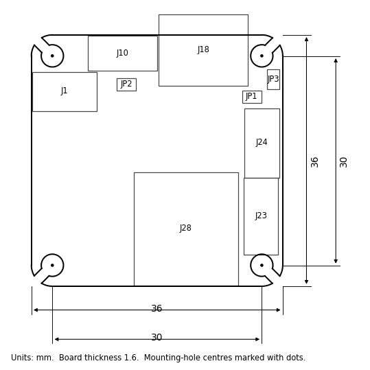
The four mounting holes lie on a 30 × 30 mm square, 3 mm in from each edge, for M3 screws or M2 screws with anti-vibration grommets; the cut-outs help when fitting the grommets. The J18 connector extends about 3 mm beyond the top edge. All dimensions in the drawings are in millimetres. The top view is the side with the micro SD socket and the STDC14 connector; the microcontroller is on the bottom side.
Absolute maximum ratings
Stresses beyond these values may cause permanent damage. They are estimated from the absolute maximum ratings of the components connected to each pin and have not been tested on the board.
| Parameter | Min | Max | Unit | Limited by |
|---|---|---|---|---|
| Supply voltage, 5V pin (J18 pin 2) | -0.3 | 7.0 | V | MCP2562FD supply |
| Voltage on CAN_H and CAN_L (DC) | -58 | +58 | V | MCP2562FD |
| Transient on CAN_H and CAN_L (ISO 7637) | -150 | +100 | V | MCP2562FD |
| ESD on CAN_H and CAN_L (HBM) | ±8 | kV | MCP2562FD |
Interfaces and connectors
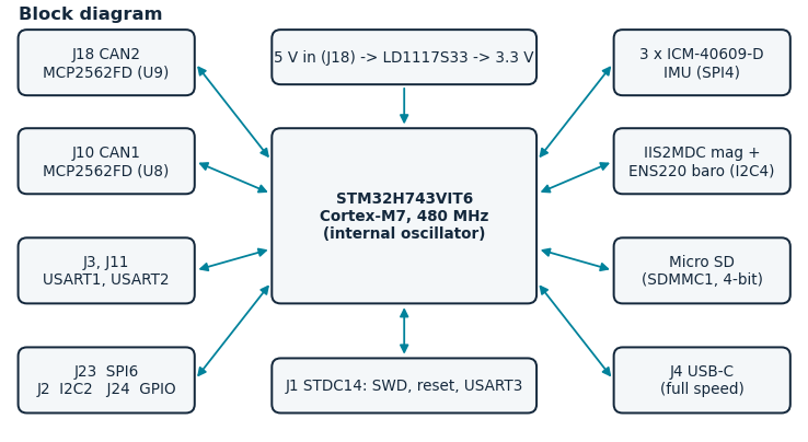
| Ref. | Function | Connector / mating part |
|---|---|---|
| J18 | Power input and CAN2 | Phoenix Contact 1844730, 2 × 3 pins, 2.54 mm pitch. Mating part: Phoenix Contact 1027605 |
| J10 | CAN1 | Molex 5055680471, 4 pins, 1.25 mm pitch. Mating part: Molex 5055650401 |
| J3 | USART1 | Molex 5055680671, 6 pins. Mating part: Molex 5055650601 |
| J11 | USART2 | Molex 5055680671, 6 pins. Mating part: Molex 5055650601 |
| J2 | I²C (I2C2) | Molex 5055680471, 4 pins. Mating part: Molex 5055650401 |
| J23 | SPI (SPI6) | Molex 5055680571, 5 pins. Mating part: Molex 5055650501 |
| J24 | GPIO | Molex 5055680471, 4 pins. Mating part: Molex 5055650401 |
| J1 | Debug and programming (STDC14) | Samtec FTSH-107-01-L-D-K, 2 x 7 pins, 1.27 mm pitch. Mating part: 14-pin STDC14 ribbon cable |
| J4 | USB | Same Sky UJ20-C-H-G-SMT-1-P16-TR, USB Type-C receptacle |
| J28 | Micro SD card | ATTEND 112L-TDA0 micro SD socket |
| JP1 | BOOT mode jumper | 2-pin header, 1 mm pitch |
| JP2, JP3 | 120 Ω CAN terminations | 2-pin headers, 1 mm pitch |
Power and CAN2 data bus (J18)
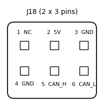
J18 carries the 5 V supply input and the CAN2 bus (FDCAN2). The 5V pins of J2, J3, J10, J11 and J23 are connected directly to this supply with no switch or current limit. The USB Type-C connector does not power the board, so the board must be powered through J18.
| Pin | Net | Type |
|---|---|---|
| 1 | NC | Not connected |
| 2 | 5V | Power input |
| 3 | GND | Power input |
| 4 | GND | Power input |
| 5 | CAN_H (CAN2_P) | I/O |
| 6 | CAN_L (CAN2_N) | I/O |
Peripheral connectors (J10, J3, J11, J2, J23, J24)
These Molex connectors bring out the CAN1 bus, two USARTs, an I²C bus, an SPI bus and four GPIO pins. All signals are 3.3 V logic except CAN. Signal names are from the point of view of the FC3 (RX is an input, TX an output).
| Pin | J10 CAN1 | J3 USART1 | J11 USART2 | J2 I²C | J23 SPI | J24 GPIO |
|---|---|---|---|---|---|---|
| 1 | GND | GND | GND | GND | GND | GPIO16 |
| 2 | CAN1_N | RTS | RTS | I2C2_SDA | SPI6_MOSI | GPIO15 |
| 3 | CAN1_P | CTS | CTS | I2C2_SCL | SPI6_MISO | GPIO14 |
| 4 | 5V | RX | RX | 5V | SPI6_SCK | GPIO13 |
| 5 | TX | TX | 5V | |||
| 6 | 5V | 5V |
Microcontroller pins: USART1 TX PA9, RX PA10, CTS PA11, RTS PA12; USART2 TX PD5, RX PD6, CTS PD3, RTS PD4; I2C2 SDA PB11, SCL PB10; SPI6 SCK PA5, MISO PA6, MOSI PA7; GPIO13 to GPIO16 PC3 to PC0. J10 is the CAN1 interface (FDCAN1); a 120 Ω termination can be added with JP2. The board has no external pull-up resistors on the I²C bus, so fit pull-ups at the connected device or in the wiring. J23 has no chip select line; use a GPIO pin if one is needed. J24 has no power pins.
Each peripheral signal of these connectors, except 5V and GND, also has a solder pad on the board, labeled with the signal name. The pads are wired in parallel with the connector pins.
| Pad | Signal |
|---|---|
| J26, J27, J29, J30 | USART1 TX, RX, CTS, RTS |
| J20, J21, J22, J25 | USART2 TX, RX, CTS, RTS |
| J5, J6 | I2C2 SDA, SCL |
| J7, J8, J9 | SPI6 MISO, MOSI, SCK |
| J16, J17 | CAN1 P, N |
| J12, J13, J14, J15 | GPIO13, GPIO14, GPIO15, GPIO16 |
Debug and programming (J1, STDC14)
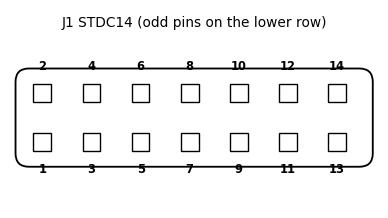
J1 is designed for use with the ST-LINK-V3MINIE and can be used to debug the board or load firmware onto the microcontroller over SWD. It also carries USART3, which gives a serial console through the ST-LINK. Mating part: 14-pin STDC14 ribbon cable.
| Pin | Signal |
|---|---|
| 3 | +3.3V |
| 4 | SWDIO |
| 5, 7, 11 | GND |
| 6 | SWCLK |
| 12 | NRST |
| 13 | USART3_TX (microcontroller output) |
| 14 | USART3_RX (microcontroller input) |
| 1, 2, 8, 9, 10 | Not connected |
Jumpers: CAN termination and BOOT mode (JP1, JP2, JP3)
120 Ω termination (JP2, JP3). Fitting a jumper on JP2 or JP3 connects a 120 Ω termination resistor across the corresponding CAN bus. JP2 terminates CAN1 (connector J10) and JP3 terminates CAN2 (connector J18). Fit a termination only on the two nodes at the ends of a bus. Jumper pitch: 1 mm.
BOOT mode (JP1). JP1 connects the BOOT0 pin of the microcontroller to 3.3 V. With a jumper fitted, resetting the board starts the microcontroller’s built-in bootloader, which can load firmware over the USB Type-C connector. For normal operation, and to run the firmware after loading it, remove the jumper before resetting the board. Jumper pitch: 1 mm.
Micro SD card (J28) and USB (J4)
Micro SD card (J28). J28 is a micro SD card socket connected to the microcontroller’s SDMMC1 peripheral in 4-bit mode (CK on PC12, CMD on PD2, D0 to D3 on PC8 to PC11), through an EMI filter. The socket has no card-detect connection. It is used for data logging.
USB (J4). J4 is a USB Type-C receptacle wired to the microcontroller’s USB OTG HS peripheral using its on-chip full-speed PHY (D+ on PB15, D- on PB14), through a common-mode choke. The CC pins have 5.1 kΩ pull-down resistors, so the board is a USB device. VBUS is only sensed (PB13); it does not power the board.
Onboard devices and buses
| Device | Bus | Microcontroller pins |
|---|---|---|
| ICM-40609-D IMU 1 (U5) | SPI4 | Chip select PB0 |
| ICM-40609-D IMU 2 (U6) | SPI4 | Chip select PE8 |
| ICM-40609-D IMU 3 (U7) | SPI4 | Chip select PE10 |
| SPI4 (shared by the IMUs) | SPI4 | SCK PE2, MISO PE5, MOSI PE6 |
| IIS2MDC magnetometer (U3) | I²C (I2C4) | SCL PD12, SDA PD13, interrupt PE15 |
| ENS220 barometer (U4) | I²C (I2C4) | SCL PD12, SDA PD13, control lines PE13 and PE14 |
| MCP2562FD CAN transceiver (U8) | FDCAN1 | RX PD0, TX PD1 |
| MCP2562FD CAN transceiver (U9) | FDCAN2 | RX PB5, TX PB6 |
The internal I²C bus (I2C4) has no external pull-up resistors on the board.
Software and firmware
The FC3 is supported by the PX4 board target efi/revA (build target efi_revA_default) in the Ether Form Inc PX4 fork. The FC3 communicates with DroneCAN (UAVCAN v0) nodes such as ESCs, servo controllers and GNSS receivers through the PX4 uavcan driver. Set the UAVCAN_ENABLE parameter to 3 to enable sensors and actuators with dynamic node ID allocation. The bus bit rate is set by UAVCAN_BITRATE (default 1000000 bit/s) and the node ID of the flight controller by UAVCAN_NODE_ID (default 1, valid range 1 to 125).
PX4 default configuration (efi/revA)
| Item | Configuration |
|---|---|
| IMUs | Three ICM-40609-D on SPI4 (icm40609d driver, one instance per chip select: PB0, PE8 and PE10) |
| Magnetometer | IIS2MDC on I2C4, address 0x1E (iis2mdc driver) |
| Barometer | ENS220S on I2C4, address 0x20 (ens220s driver) |
| DroneCAN | Two interfaces (CAN1 and CAN2), PX4 uavcan driver |
| RC input | Spektrum DSM receiver on USART2 (J11) |
| USB | USB Type-C, full speed, using the on-chip OTG_HS PHY (PB14, PB15; VBUS sensed on PB13). Provides the PX4 CDC/ACM serial port for MAVLink and the shell |
| External I²C (J2) | I2C2 is enabled as an external bus. The board has no pull-ups, so the connected device must provide them |
| External SPI (J23) | SPI6 is enabled as an external bus. No chip select is assigned because J23 has none |
| USART1 (J3) | Pins PA9 (TX) and PA10 (RX) are configured. Hardware flow control is not enabled |
| GPIO (J24) | GPIO13 to GPIO16 are configured as inputs at start-up and can be read or driven with the gpio command |
| SD card | Logging to the micro SD card (SDLOG_BACKEND bit 0, enabled by default) |
Programming: connect an ST-LINK-V3MINIE to J1 (STDC14) to load firmware or debug over SWD. Firmware can also be loaded over the USB Type-C connector by fitting the BOOT jumper (JP1) and resetting the board.
Resources
- Firmware source code and binaries: github.com/Ether-Form-Inc
- DroneCAN specification: CAN bus transport layer
- DroneCAN message definitions: DroneCAN DSDL (uavcan)
Request a quote or discuss your integration
Choose the inquiry type that fits. A standard bulk quote only needs a quantity and your contact details; engineering and customization inquiries need a short description of what you need.